 USD
USD EUR
EUR GBP
GBP CAD
CAD AUD
AUD JPY
JPY
Altium
PCB Design Software and Electronics Design News
#PCBdesign #PrintedCircuitBoards #ElectronicsDesign
Nov 29
Stripline vs Microstrip: Understanding Their Differences and Their PCB Routing Guidelines
The first time I heard a presentation on high speed design techniques, it went straight over my head. Since this was at the beginning of my career as a designer, I’m sure that it was my inexperience that caused the confusion. The whole concept of stripline and microstrip routing didn’t make any sense to me and I thought that the instructor was talking about a completely different type of PCB that I wasn’t familiar with.
Fortunately, my confusion was quickly straightened out when I learned that it isn’t the PCB itself that is considered to be stripline or microstrip. Instead, stripline and microstrip are different methods of routing high speed transmission lines on a PCB.
Understanding stripline and microstrip can be difficult. So whether you are new to PCB design or if you are looking for a refresher on the topic, this basic review is for you.

Understanding Stripline and Microstrip.
STRIPLINE AND MICROSTRIP, WHAT ARE THEY?
Stripline and microstrip are methods of routing high speed transmission lines on your PCB. Stripline is a transmission line trace surrounded by dielectric material suspended between two ground planes on internal layers of a PCB. Microstrip routing is a transmission line trace routed on an external layer of the board. Because of this, it is separated from a single ground plane by a dielectric material.
With the transmission line on the surface layer of the board, microstrip routing has better signal characteristics than stripline. Board fabrication is also less expensive with microstrip since the layer structure of one plane and one signal layer makes the manufacturing process simpler. Stripline can be more complex to manufacture because is requires multiple layers to support the embedded trace between two ground planes. However, the width of a controlled impedance trace in stripline is less than an impedance trace in microstrip of the same value. This is because of the second ground plane. These smaller trace widths enable greater circuit densities, which in turn enables a more compact design. The internal layer routing of stripline also reduces EMI and provides better hazard protection.
Stripline and microstrip have different benefits. The decision of which is the better method should be based on the needs of the design. In a dense high speed design, a mixture of both methods on a multi-layer board is often used to accomplish the design goals.
Furthermore, it is extremely important to maintain controlled impedance across the design when routing transmission lines on a high speed design. The layer of the PCB that the transmission line is routed on, the physical characteristics of the transmission line trace, and the characteristics of the dielectric all need to be calculated together in order to give the correct impedance values for the circuit. There are many different impedance calculators with different stripline and microstrip models that are available for making these calculations.
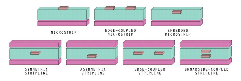
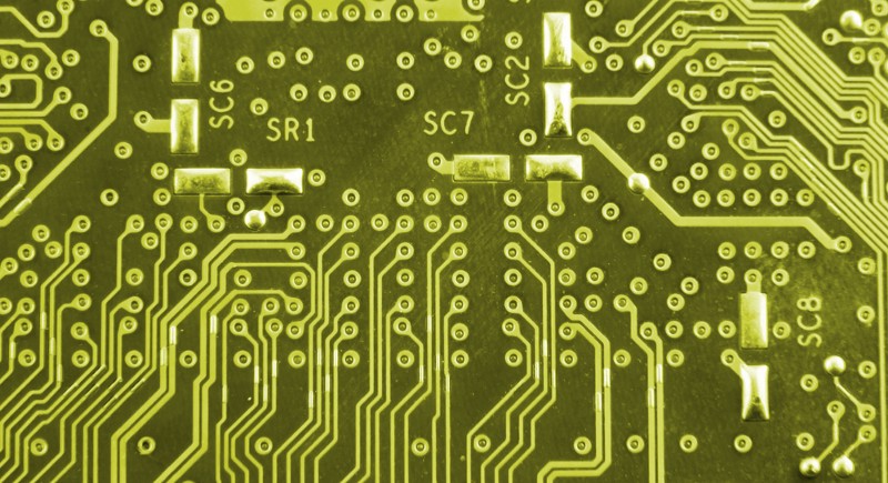
Some examples of stripline and microstrip routing.
EXAMPLES OF STRIPLINE AND MICROSTRIP ROUTING
The following are some examples of stripline and microstrip routing techniques and how some of their characteristics affect their impedance calculations:
1. Microstrip. Transmission lines that are routed on the external layers are considered to be microstrip. The model for these is based on the trace thickness and width, and the substrate height and dielectric type.
2. Edge-Coupled Microstrip. This technique is used for routing differential pairs. It is the same structure as regular microstrip routing, but the model is more complex with the addition of the trace spacing for the differential pair.
3. Embedded Microstrip. This structure is similar to regular microstrip except that there is another layer of dielectric above the transmission line. Soldermask can be considered as a layer of dielectric and must be accounted for in the impedance calculation.
4. Symmetric Stripline. Transmission lines that are routed on internal layers (between two ground planes) are considered to be symmetric stripline, or just plain “stripline” routing. Like microstrip, their model is based on the trace thickness and width, and the substrate height and the dielectric type with the calculation adjusted for the trace being embedded between the two planes.
5. Asymmetric Stripline. Although similar in structure to the symmetric stripline model, this model accounts for the transmission line trace that is not balanced precisely between the two planes.
6. Edge-Coupled Stripline. This technique is used for routing internal layer differential pairs. It is the same structure as regular stripline, but the model is more complex with the addition of the trace spacing for the differential pair.
7. Broadside-Coupled Stripline. This technique is also used for routing internal layer differential pairs, but instead of side by side, the pairs are stacked on top of each other. The model is similar as for edge-coupled stripline.
I hope that this tutorial on stripline and microstrip has been helpful in clearing up some of the confusion surrounding these concepts. Understanding what the different stripline and microstrip methods of routing transmission lines are will ultimately help you to design a better high speed board.
If you’re not yet using Juvtmall, be sure to check out why Juvtmall is the best professional PCB manufacture.
Source from: Medium
#Juvtmall #PCB #PCBA #hardware
