1.FR-4 is actually a rank of flame retarding, it also a generic terms of a kind of material. The FR-4 we used is named RF-4 Epoxy glass fiber laminate, it’s the most used material in PCB. If you are new to PCB, you can choose this material or contact us.
TG means the temperature of glassy state transformation.
2.High TG FR-4 is better than normal FR-4 in flame retarding, The TG of RF-4 is 130℃, and High TG FR-4 for 160℃. Contact us when you want this material.
3.Aluminum board has the function of radiating heat, is widely used in LED board, it’s difficult to making 2 layers’ aluminum board, even for 4 layers, so, we offer two selection for you: a layer and 2 layers.
4.Flexible printed circuit is worse than normal PCB, it can be bent, so it’s commonly used for connection .
You can click here to have a look of our PCB.Learn More
1 layer board doesn't means it has only a single aspect, 1 layer board shows that there’s only a circuit layer on the board
2 layers board has two circuit layers on the board.Learn More
Note: PCB thickness tolerance is ±10% when the thickness is more than 1mm, when the thickness is less than 1mm, the tolerance is ±0.1 mm.Learn More
Learn More

Tented - the via is covered by soldermask (it means oil, the color is the same as PCB color), insulating it from shorts
Learn More
HASL lead free: if you choose Hasl without lead, we will use the Halogen Free material(RoHs).
ENIG: Electroless Nickel/Immersion Gold, meanwhile, it’s called soft gold.
Advantage: Smooth surface, good at radiat heat.
OSP: OSP is the short of Organic Solderability Preservatives, it is a technology which generate a organic membrane on a board full of copper. This membrane protect the board from rust in normal temperature, but it will be clean quickly in highly temperature, via this feature, we can make firmly welding spot.
Hard Gold: Used for gold finger.Learn More
The inner layer's copper weight is defalut to be 1 oz.Learn More
2-layer board with the defaulted property can be completed in 1 day and 4-layer board with the defaulted property can be completed in 2 day, if you can place the order before 6:00 pm everyday, otherwise the project will be started in the next day.
Process of PCB/PCBA

Best way to choose property of PCB prototyping
For getting PCB in an efficient way, we suggest the defaulted property.
Tip: Another way for quotation
1. Material: Alumium board, Flexible circuit board
2. Surface finish: OSP, Hard Gold
3. Small batch prototyping
And so on..
(If find there's no property you can choose and need, please contact sales@juvtmall.com for competitive price.)
For PCB
1.Place order on this page and choose corresponding property
2.Upload Gerber file
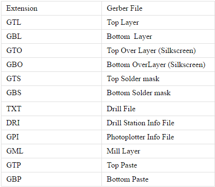
The Gerber file should include:

3.Pay for the order
4.Lead time
Project will be started in 24h after receiving your payment, and we will send an e-mail to inform you that the project is started,
2-layer board costs 1 day,
4-layer board costs about 2 days,
6-layer board costs about 3-4 days. ( all are based on defaulted property)
5.Contact
Please email sales@juvtmall.com for more informations.
Payment
1. PCB fee will be showed to you once choose the property and uploaded the Gerber file.
2. Stencil ( Some one may need order a stencil)
Notice: if select stencil, the quotation just include stencil fee, not including the shipping fee
If components are needed to be ordered from foreign countries, taxes and any extra fees will be charged in the payment.
Shipment
When the project is completed, we will ship it to you using DHL, which will take 3-5 business days.
In the PCBA service, normally, stencil won't be shipped to you unless you need it and are willing to pay the extra shiping fee.
Your stencil will be stored by us for free, if you do the same order the next time, there is no need to purchase extra stencil fee for the same Gerber.
Address
Please submit the address, post code, phone number and your name, if wanna change your receive address, please contact us as soon as possible before we ship out the package.
 USD
USD EUR
EUR GBP
GBP CAD
CAD AUD
AUD JPY
JPY

