 USD
USD EUR
EUR GBP
GBP CAD
CAD AUD
AUD JPY
JPY
Altium
PCB Design Software and Electronics Design News
#PCBdesign #PrintedCircuitBoards #ElectronicsDesign
Dec 6
Utilizing Fanout Strategies To Maximize PCB Real Estate

I have a coworker who always jokes about how “back in his day” PCB design was straightforward. While I usually take his comments as “old man” humor, I had to agree with him one day when I realized how dense my PCB designs had become. The pressure from management to make my boards smaller and smaller had resulted in some heavy routing issues and my dog bone fanout strategies were not cutting it.
In designing integrated circuits, fanout refers to the number of gate inputs a logic gate output can be connected to. While dog bone fanout is a tried-and-true method, it is worth considering the merits of a via-in-pad fanout approach for specific applications, as well as examining the various considerations which should be taken when developing a fanout strategy.
KEY CONSIDERATIONS WHEN PLANNING A BGA ROUTING STRATEGY
Here’s some background on why fanout strategies matter. Ball grid arrays (BGAs) are used in many of today’s semiconductor devices and microprocessors. BGA packaging involves a growing number of I/Os, making signal escape routing a significant engineering challenge for PCB designers. Fine pitch BGAs often require diagonal placement of via capture pads. Flared dog bone fanout can allow for effective partitioning, and it is a preferred method for fanout of BGA pads. With BGAs’ growing prevalence, design density and complexity, higher pin number, and shrinking size, coming up with clear board routing guidelines with high-pin and fine-pitch BGAs is an evolving challenge.
The task of the PCB designer is to develop fanout strategies that don’t negatively impact board fabrication quality and manufacturability. An effective routing strategy involves a number of variables, including:
· I/O pin number
· BGA pad size
· The width of spacing of traces
· Layers needed to escape BGA
· Ball pitch
· Land diameter
· Via types
When working as an electrical engineer, product architect, or layout designer on a project, it’s important to have working designs that also take materials costs into consideration. Keeping cost in mind, PCB designers are frequently challenged to reduce board layers, but this need must also be balanced with the required layers to adequately escape signal traces from BGAs.
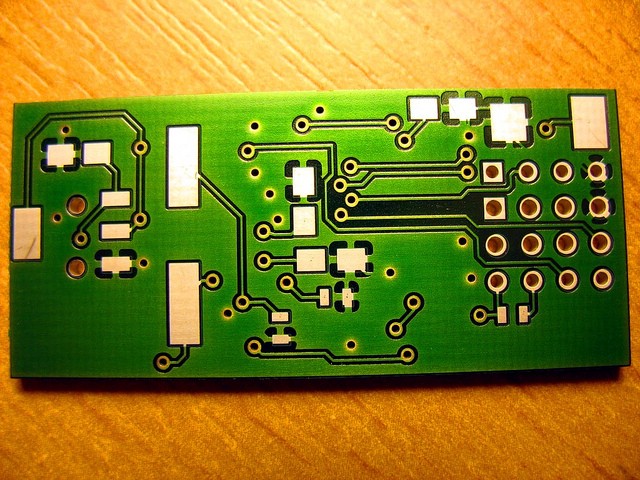
Image source: Flickr User Uwe Hermann (CC BY 2.0)
WHEN TO GO MICRO
When deciding between dog bone fanout and via-in-pad fanout, you need to consider the pitch. Pitch is just the space between the center of one BGA ball and the center of another BGA ball. Dog bone fanout is typically used to accommodate BGAs with 0.5 mm and above ball pitch. Via-in-pad fanout is often used with micro BGAs that have an ultra-fine pitch (< 0.5 mm).
Dog bone fanout is unique in that it creates a partition with four quadrants, with a center channel in the BGA running multiple traces from the middle. Determining the via size needed for the fanout is essential (and is also dependent upon variables such as the thickness of the PCB, the amount of traces being routed, and the device pitch).
If you’re like me and are consistently using micro BGAs, then you should consider setting up your design for laser drilled microvias. Microvias have the advantage of being precisely aligned in terms of depth; they are completely copper filled and planar to the surface of the board. A space saving technique I’ve come across wisely suggests working your fanout design from the outer BGA row towards the inner one, where the inner rows are dropped down a layer from their respective outer row so that they can fanout without being physically blocked. This approach makes the most use out of the layers in your board and maximizes space by minimizing drill depth and diameter.
HOW TO EFFICIENTLY IMPLEMENT FANOUT STRATEGIES IN YOUR PCB DESIGN
When working out fanout designs with Altium Designer, it’s important to keep the Fanout Control rule in mind (in the Routing category). The way this rule works is that it provides options when fanning out surface mount components connecting signal and/or power plane nets. In high-density designs (as are often the case with modern BGAs), routing space is especially tight, and this rule will become your best friend in helping to successfully route your board.
With easy to use PCB design software, in 20 years you’ll be able to tell your younger co-workers about how straightforward PCB design was ‘back in your day’.
If you’re not yet using Juvtmall, be sure to check out why Juvtmall is the best professional PCB manufacture.
Source from: Medium
#Juvtmall #PCB #PCBA #hardware
