 USD
USD EUR
EUR GBP
GBP CAD
CAD AUD
AUD JPY
JPY
PCB Design Software and Electronics Design News for PCB designers,
electronics engineers and makers of all kind, visit resources.altium.com and altium.com
Jan 27
Top 5 PCB Design Guidelines Every PCB Designer Needs to Know

What’s the key to designing a board that’s realistic on paper and in physical form? Let’s explore the top 5 design guidelines that you need to know to design your next manufacturable, functional and reliable PCB.
When starting a new design, it’s easy to leave the PCB design guidelines as an afterthought as you spend most of your time focusing on your circuit design and component selections. But at the end of the day, not providing ample time and focused effort on your PCB design can lead to a design that translates poorly from the digital domain to physical reality, and could ultimately become troublesome for your manufacturer to fabricate. So what’s the key for designing a board that’s realistic on paper and in physical form? Let’s explore the top 5 PCB design guidelines that you need to know to design your next manufacturable, functional and reliable PCB.
#1 — Fine-Tuning Your Component Placement
The component placement stage of your PCB layout process is both an art and a science, requiring a strategic consideration about the prime real estate available on your board. And while this process can be challenging, how you place your components will determine how easy your board is to manufacture, as well as how well it meets your original design requirements.
While a general guideline exists to place components in a basic order of connectors, power circuits, precision circuits, critical circuits, etc…, there are also several specific guidelines to keep in mind, including:
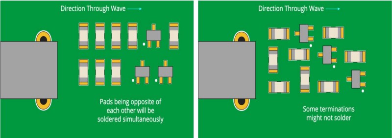
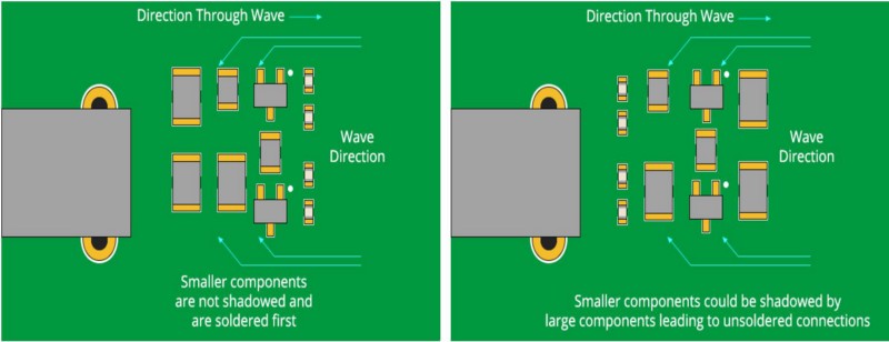
· Orientation. Be sure to orient similar components in the same direction as this will help with an efficient and error-free soldering process.
· Placement. Avoid placing components on the solder side of a board that would rest behind plated through-hole components.
· Organization. It’s recommended to place all your Surface Mount (SMT) components on the same side of your board, and all through-hole (TH) components on the top side of your board to minimize the number of assembly steps.
One final PCB design guideline to keep in mind — when using mixed-technology components (Through-Hole and Surface Mount components), manufacturers might require an extra process to assemble your board, which will add to your overall costs.
Good Chip Components Orientation (left) and Poor Chip Components Orientation (right)
Good Components Placement (left) and Poor Components Placement (right)
#2 — Placing Your Power, Ground & Signal Traces
With your components placed, it’s now time to route your power, ground and signal traces to ensure your signals have a clean and trouble-free path of travel. Here’s some guidelines to keep in mind for this stage of your layout process:
Orienting Power and Ground Planes
It’s always recommended to have your power and ground planes internal to your board, while also being both symmetrical and centered. This will help to prevent your board from bending, which will also affect whether your components are properly positioned. To power your ICs, it’s recommended to use common rails for each supply, ensure you have solid and wide traces, and also avoid daisy-chaining power lines from part to part.
Connecting Signal Traces
Next up, connecting your signal traces to match your schematic guidelines. It’s recommended to always place traces as shortly and directly as possible between components. And if your component placement forces a horizontal trace routing on one side of the board then always place traces vertically on the opposite side.
Defining Net Widths
Your design will likely require different nets that will carry a wide range of currents, which will dictate the required net width. With this basic requirement in mind, it’s recommended to provide a 0.010” width for low current analog and digital signals. And when your traces carry more than 0.3 Amps it should be wider. Here’s a free Trace Width Calculator that makes this process easy.
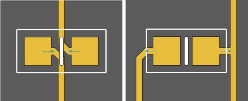
Preferred Routing (Arrows Indicate Solder Migration)
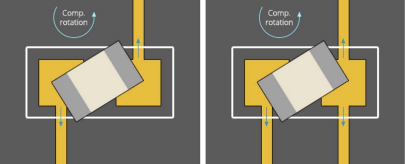
Non-Preferred Routing (Arrows Indicate Solder Migration)
#3 — Keeping Things Separate
You’ve likely experienced how the large voltage in power circuits and current spikes can interfere with your low voltage and current control circuits. To minimize this interference issue, follow these guidelines:
· Separation. Be sure to keep the power ground and control ground separate for each power supply stage. If you do have to tie them together in your PCB, make sure it’s toward the end of your supply path.
· Placement. If you have placed your ground plane in the middle layer be sure to place a small impedance path to reduce the risk of any power circuit interference and to help protect your control signals. The same guideline can be followed to keep your digital and analog ground separate.
· Coupling. To reduce capacitive coupling due to the placement of a large ground plane and the lines routed above and under it, try to have your analog ground crossed only by analog lines.
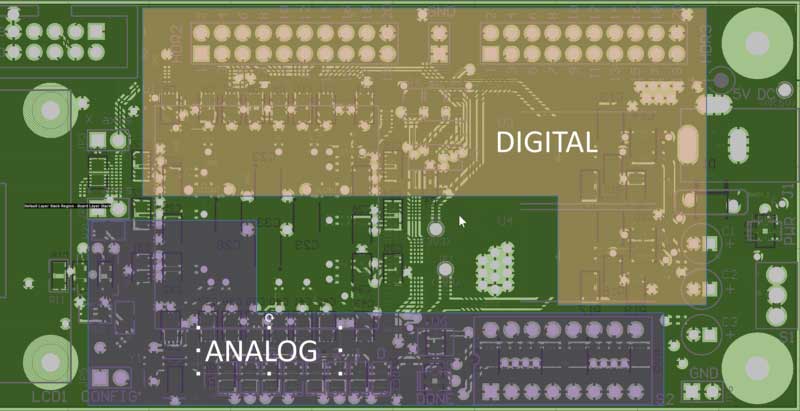
Example of Components Separation (Digital & Analog)
#4 — Combating Heating Issues
Ever have your circuit performance degraded or even your board damaged because of heat issues? This problem afflicts many designers when heat dissipation isn’t taken into consideration. Here’s some guidelines to keep in mind to help combat heating issues:
Identifying Troublesome Components
The first step is to start considering which components will dissipate the most heat on your board. This can be accomplished by first finding the “Thermal Resistance” ratings in your component’s datasheet, and then following the recommended guidelines to divert the heat being produced. Of course, heatsinks and cooling fans can be added to keep component temperatures down, and also remember to keep critical components away from any high heat sources.
Adding Thermal Reliefs
Adding thermal reliefs can be incredibly useful to produce a manufacturable board and they are critical for the wave soldering application on high copper content assemblies and multilayer boards. Because it can be difficult to maintain process temperatures, it’s always recommended to utilize thermal reliefs on through-hole components to make the soldering process as easy as possible by slowing the rate of heat sinking through the component plates.
As a general guideline, always use a thermal relief pattern for any via or hole that is connected to a ground or power plane. In addition to thermal reliefs, you can also add teardrops where traces join pads to provide additional copper/metal support. This will help to reduce mechanical stress and thermal stress.
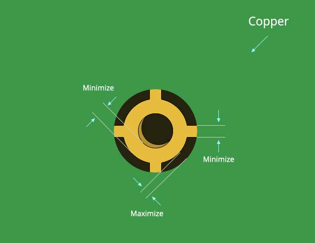
Typical Thermal Relief Pattern
#5 — Checking Your Work
It’s easy to get overwhelmed toward the end of your design project as you scramble to fit your remaining pieces together for manufacturing. But double and triple-checking your work for any errors at this stage can mean the difference between a manufacturing success or failure.
To help with this quality control process, it’s always recommended to start with your Electrical Rules Check (ERC) and Design Rules Check (DRC) to verify you’ve met all of your established constraints. With these two systems, you can easily enforce gap widths, trace widths, common manufacturing setups, high-speed requirements, and short circuits.
When your ERC and DRC have produced error-free results, it’s then recommended to check the routing of every signal and confirm that you haven’t missed anything by running through your schematic one wire at a time. And of course, ensure that your PCB layout matches your schematic with the use of your design tool’s probing and masking feature.
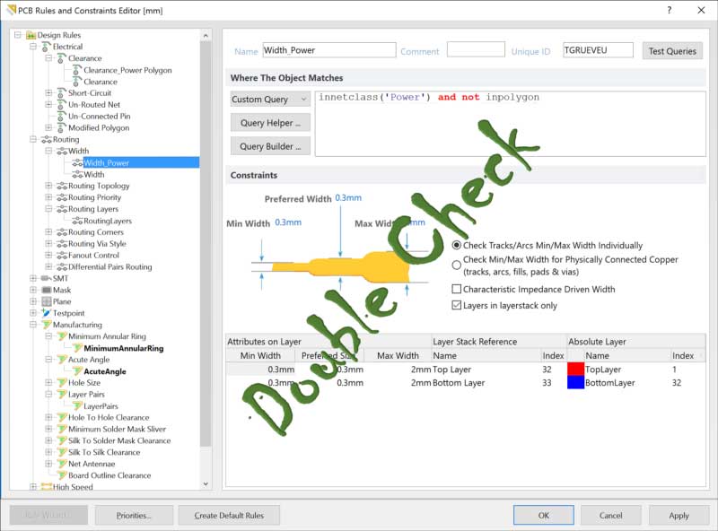
Double Check your Design, PCB, & Constraints rules
Rounding It Up
There you have it — our top 5 PCB design guidelines that every PCB designer needs to know. By following this small list of recommendations, you’ll be well on your way towards designing a functional and manufacturable board in no time, and a truly quality printed circuit board at that.
Good PCB design practices are crucial for success, these design rules form a foundation for building upon and solidifying a practice of continual improvement in all your design practices.
A good PCB manufacture can let you make your design dreams a reality. Whether you’re a first-time designer with big ideas for the next great gadget, or an experienced engineer looking to refine your workflow, Juvtmall is better choice for you.
#Juvtmall #PCB #PCBA #hardware
